2026 / 07 / 21
RZ/N2L SDRAM由CS2改为CS3相应PN代码修改方法
瑞萨RZ/N2L MPU
RZ/N2L是一种工业以太网通信用MPU,可轻松将网络功能添加到工业设备中。它搭载支持TSN的三端口千兆以太网交换机和EtherCAT®从控制器,可支持EtherCAT、PROFINET RT/IRT、EtherNet/IP™、OPC UA等主要的工业以太网通信协议。它对网络专用配套芯片加以优化,无需大幅改变设备的内部配置即可直接连接并快速访问外部应用主机CPU。此外,Arm® Cortex®-R52的最大工作频率为400MHz,外设功能包括带ECC的大容量RAM与ΔΣ I/F、A/D转换器、PWM定时器、UART和CAN等,可在单个芯片上实现远程I/O、传感器集线器、变频器和网关。
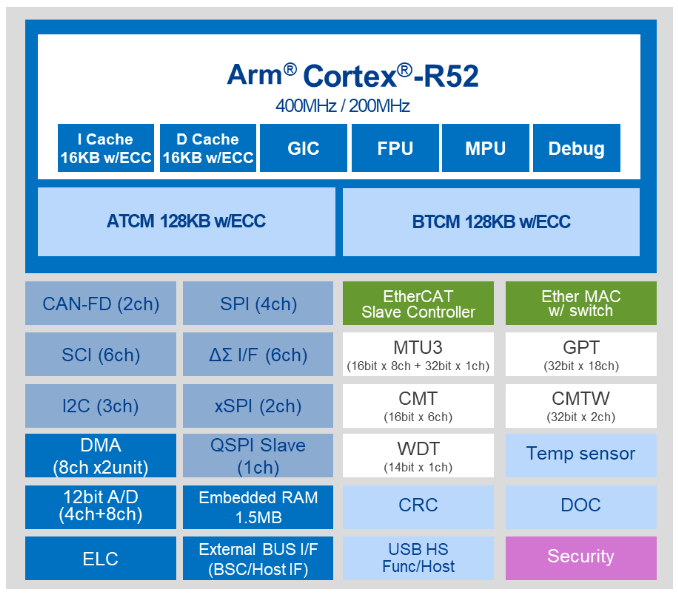
RZ/N2L:https://www.renesas.cn/cn/zh/products/microcontrollers-microprocessors/rz-mpus/rzn2l-integrated-tsn-compliant-3-port-gigabit-ethernet-switch-enables-various-industrial-applications
RZ/N2L PN例程,SDRAM接口片选使用的是CS2(因为RZN2L RSK 的特殊硬件设计),而根据UM,系统里使用单片SDRAM的话,BSC必须CS3#。本文将为您演示为了适配使用CS3的硬件要求,PN的代码需要做的三处修改。
修改 hal_entry.c 文件中 bsp_sdram_init() 函数,把与CS2相关的配置屏蔽掉,如下面代码所示。
#if 0 ~ #endif 之间代码,60~86行:
static void bsp_sdram_init (void)
{

    volatile uint32_t val;

    R_RWP_S->PRCRS  = 0x0000A50F;
    R_RWP_NS->PRCRN = 0x0000A50F;

    /* NOTE: Port setting and CKIO configuration should have been done before */

    // Configure clock frequency
    val = R_SYSC_NS->SCKCR;
    val &= ~(7<<16);
    //val |=  (6<<16);// CKIO clock: 25MHz
    val |=  (1<<16);// CKIO clock: 66.7MHz
    R_SYSC_NS->SCKCR = val;

    /* Enable BSC and CKIO module */
    val = R_SYSC_NS->MSTPCRA;
    val &= ~(1<<0);
    R_SYSC_NS->MSTPCRA = val;
    val = R_SYSC_NS->MSTPCRA;        // dummy read: step1

    // Enable CKIO module
    val = R_SYSC_NS->MSTPCRD;
    val &= ~(1<<11);
    R_SYSC_NS->MSTPCRD = val;
    val = R_SYSC_NS->MSTPCRD;        // dummy read: step1

    R_RWP_NS->PRCRN = 0x0000A500;
    R_RWP_S->PRCRS  = 0x0000A500;

    /* Wait */
val = R_BSC->CSnBCR[3];        // dummy read: step2
val = R_BSC->CSnBCR[3];        // dummy read: step2
val = R_BSC->CSnBCR[3];        // dummy read: step2
val = R_BSC->CSnBCR[3];        // dummy read: step2
val = R_BSC->CSnBCR[3];        // dummy read: step2

    /* SDRAM:W9825G6KH-6 */
    /* Row address: A0-A12. Column address: A0-A8. */
val = ( 2 <<  9)// BSZ: data bus witdh: 16-bits
 | ( 1 << 11)// Reserved
 | ( 4 << 12)// TYPE: SDRAM
 | ( 0 << 16)// IWRRS: Idle State Insertion between Read-Read Cycles in the Same CS Space
 | ( 0 << 19)// IWRRD: Idle State Insertion between Read-Read Cycles in Different CS Spaces
 | ( 0 << 22)// IWRWS: Idle State Insertion between Read-Write Cycles in the Same CS Space
 | ( 0 << 25)// IWRWD: Idle State Insertion between Read-Write Cycles in Different CS Spaces
 | ( 0 << 28);// IWW: Idle Cycles between Write-Read Cycles and Write-Write Cycles
    R_BSC->CSnBCR[3] = val;

    /* Wait cycle */
val = ( 2 <<  0)// WTRC: Number of Idle states frmo REF Command/Self-refresh relase to ACTV/REF/MRS command
 | ( 2 <<  3)// TRWL: Number of Auto-precharge startup Wait Cycle
 | ( 1 <<  7)// A3CL: CAS Latency: 2
 | ( 1 << 10)// WTRCD: Number of Waits between ACTV command and READ/WRIT command
 | ( 1 << 13);// WTRP: Number of Auto-precharge completion wait states
        R_BSC->CS3WCR_1 = val;

#if 0
    /* Wait */
val = R_BSC->CSnBCR[2];        // dummy read: step2
val = R_BSC->CSnBCR[2];        // dummy read: step2
val = R_BSC->CSnBCR[2];        // dummy read: step2
val = R_BSC->CSnBCR[2];        // dummy read: step2
val = R_BSC->CSnBCR[2];        // dummy read: step2


    /* SDRAM:W9825G6KH-6 */
    /* Row address: A0-A12. Column address: A0-A8. */
val = ( 2 <<  9)// BSZ: data bus witdh: 16-bits
 | ( 1 << 11)// Reserved
 | ( 4 << 12)// TYPE: SDRAM
 | ( 0 << 16)// IWRRS: Idle State Insertion between Read-Read Cycles in the Same CS Space
 | ( 0 << 19)// IWRRD: Idle State Insertion between Read-Read Cycles in Different CS Spaces
 | ( 0 << 22)// IWRWS: Idle State Insertion between Read-Write Cycles in the Same CS Space
 | ( 0 << 25)// IWRWD: Idle State Insertion between Read-Write Cycles in Different CS Spaces
 | ( 0 << 28);// IWW: Idle Cycles between Write-Read Cycles and Write-Write Cycles
    R_BSC->CSnBCR[2] = val;

   /* Wait cycle */
    val = ( 1 <<  7)// A3CL: CAS Latency: 2
 | ( 1 << 10);// Reserved 1

    R_BSC->CS2WCR_1 = val;
#endif
    /* SDRAM control */
    R_BSC->SDCR = 0x00110811;// auto-refresh, auto-precharge mode, Col 9-bits, Row 13-bits

    /* Refresh setting for SDRAM */
    R_BSC->RTCOR = BSC_PROTECT_KEY
                 | ( 29 <<  0);        // Refresh Time: 29 counts
    R_BSC->RTCSR = BSC_PROTECT_KEY
                 | (  0 <<  7)         // Compare match Flag: clear
                 | (  0 <<  6)         // Compare match interrupt enable: Disabled
                 | (  2 <<  3)         // Refresh timer count clock: CKIO/16
                 | (  0 <<  0);        // Refresh count: 1 time

    /* wait 200us*/
    R_BSP_SoftwareDelay(200, BSP_DELAY_UNITS_MICROSECONDS);

    /* Power-on Sequence */
    /* Set mode register of SDRAM. needs wait for 2 SDRAM clock after set. */
    *((uint16_t *)0x80212040) = 0x0000;   // Burst length=1, Sequential, CL=2, Burst read and burst write
    *((uint16_t *)0x80211040) = 0x0000;   // Burst length=1, Sequential, CL=2, Burst read and burst write

}
pnip_reg.h 头文件,将CS2 Region的地址定义修改为CS3的Memory Region,如下图将0x54xxxxxx地址修改为0x58xxxxxx地址。
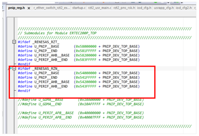
#ifdef _RENESAS_RZN_
#define U_PNIP__BASE       (0x58000000 + PNIP_DEV_TOP_BASE)
#define U_PNIP__END        (0x581FFFFF + PNIP_DEV_TOP_BASE)
#define U_PERIF_AHB__BASE  (0x58200000 + PNIP_DEV_TOP_BASE)
#define U_PERIF_AHB__END   (0x583FFFFF + PNIP_DEV_TOP_BASE)
#endif
修改Linker文件中SDRAM Adddress相关Region定义。
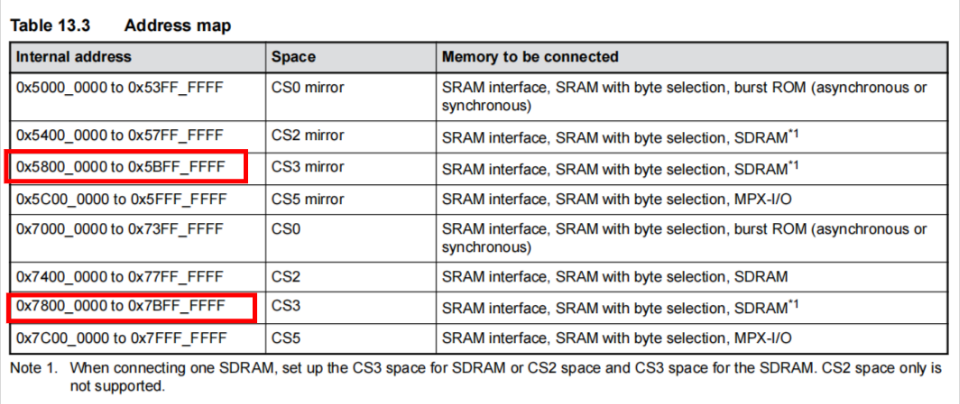
以IAR的 fsp_xspi0_boot.icf 为例:
文件中定义了
地址空间为:0x7440 0010 – 0x744F FFFF;
需要修改为:0x7840 0010 - 0x784F FFFF;
地址空间为:0x5500 0000 – 0x555F FFFF;
需要修改为:0x5900 0000 – 0x595F FFFF;
地址空间为:0x5450 0000 – 0x547F FFFF;
需要修改为:0x5850 0000 – 0x587F FFFF;










 样品
样品 应用
应用 微信
微信
